I’ve moved on a bit since the last time I looked at logic gates so I think it’s about time to revisit…
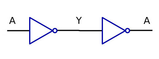
I’ve found out a bit more on NOT gates, they are actually called inverters, not surprisingly as they ‘invert’ the input into the output. When you connect up two inverters in series you get a ‘buffer. All this does is take the output of the first NOT gate and feeds it into the input of the next one. The two cancel each other out so you the final output is the same as the first input:
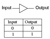
Possibly pointless? Not really, it does have a practical use. Logic gate circuits are signal amplifiers (remember logic gates are made up of those lovely signal boosting transistors…), a weak signal can be boosted using this combination of two inverters. The logic level isn’t changed, you still get a high output from a high input but the final signal is stronger than the initial one. The symbol is the same as for a NOT gate just without the little bubble on the end.
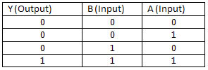
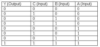
With additional inputs logic gates can process more complex information, for example a 2 input gate has 4 output possibilities, a 3 input gate has 8 output possibilities etc.
The equation for working out number of possibilities is…
Number of possible input states = 2n
Where n = number of inputs
This means that your gates can control much more complex systems.
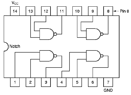
I had a go at prototyping a logic gate circuit using a NAND gate chip but first I should probably say how to interpret/draw logic gates in circuit diagrams. You can do it in one of two ways either by drawing in the IC (labeling it with the chip number) and numbering the pins:
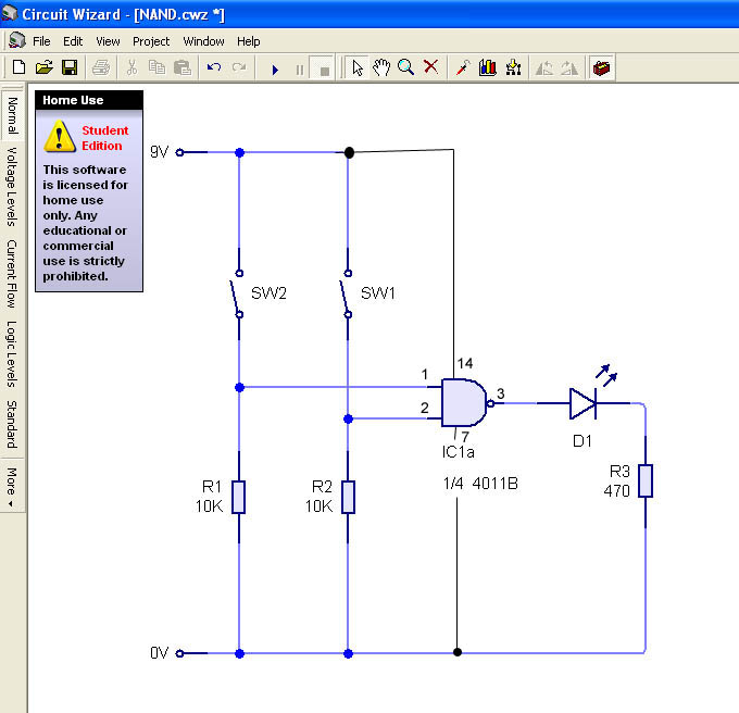
Or by using the logic gate symbol and labeling the inputs and outputs. The label on the symbol below indicates that it is 1/4 of a 4011 chip, so only using one of the 4 NAND gates contained in this chip.
(Please excuse the clumsy editing, I couldn’t find how to edit the circuit symbol in circuit wizard…)
Here’s my circuit in action:
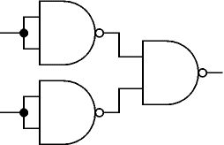
I also found out that NAND and NOR gates have a cool capability, they are universal gates. This means that by arranging NAND and NOR gates in specific ways you can get them to mimic any other gate:
So to make an OR gate you need to connect up the gates in your IC like this:
(All truth tables can be found here)
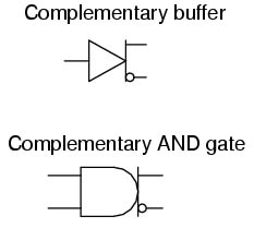
There are also complementary output gates, this basically means that you have a gate that can produce inverted and non-inverted outputs. So you could have an AND gate that could give you an AND gate out put or a NAND gate output:
So why would you need a gate that can do this if you could just hook up a NOT gate off the output lead? For two reasons, 1) it saves space and 2) adding in a seperate NOT causes a time delay so if your inputs were alternating high and low your non-inverted output and your inverted outputs would change at slightly different times.
Again this is getting a bit far afield from what I’m aiming for but would be interesting to look at in the future.
